 All About News Trusted news and information
optimized 3nm technique achieves 45% decreased power usage, 23% stepped forward performance and sixteen% smaller floor area compared to 5nm method
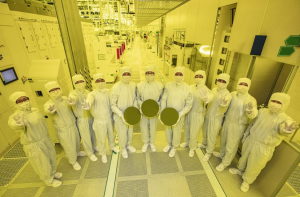
samsung electronics, the arena leader in semiconductor era, nowadays announced that it has started initial production of its three-nanometer (nm) process node making use of gate-all-around (gaa) transistor architecture.
multi-bridge-channel fet (mbcfet™), samsung’s gaa generation implemented for the first time ever, defies the performance boundaries of finfet, enhancing strength efficiency by using decreasing the deliver voltage degree, even as also improving overall performance by using growing power cutting-edge functionality.
samsung is beginning the primary application of the nanosheet transistor with semiconductor chips for high performance, low power computing application and plans to make bigger to cellular processors.
“samsung has grown unexpectedly as we keep to demonstrate leadership in applying subsequent-era technology to manufacturing, consisting of foundry enterprise’s first high-k metal gate, finfet, in addition to euv. we are seeking to continue this leadership with the arena’s first 3nm process with the mbcfet™,” said dr. siyoung choi, president and head of foundry business at samsung electronics. “we can keep active innovation in competitive generation development and build procedures that help expedite attaining adulthood of technology.”

design-technology optimization for maximized ppa
samsung’s proprietary era utilizes nanosheets with wider channels, which allow better overall performance and extra electricity efficiency compared to gaa technology the usage of nanowires with narrower channels. utilizing the 3nm gaa generation, samsung might be able to adjust the channel width of the nanosheet as a way to optimize energy utilization and performance to fulfill numerous consumer desires.
similarly, the layout flexibility of gaa is notably effective for design technology co-optimization (dtco),1 which allows improve energy, performance, area (ppa) blessings. compared to 5nm technique, the first-technology 3nm process can reduce power consumption by means of as much as forty five%, improve performance via 23% and decrease location by using sixteen% as compared to 5nm, at the same time as the second one-generation 3nm system is to lessen energy intake through up to 50%, improve overall performance through 30% and decrease location by way of 35%.
supplying 3nm design infrastructure & offerings with safe™ companions
as technology nodes get smaller and chip performance wishes grow more, ic designers face demanding situations of managing awesome amounts of information to confirm complicated products with extra functions and tighter scaling. to satisfy such demands, samsung strives to offer a extra strong layout environment to assist reduce the time required for design, verification and sign-off method, whilst additionally boosting product reliability.
since the third area of 2021, samsung electronics has been presenting confirmed layout infrastructure thru enormous practise with samsung superior foundry surroundings (safe™) partners which includes ansys, cadence, siemens and synopsys, to assist clients perfect their product in a reduced period of time.
quotes from safe™ partners
ansys, [john lee, vp and standard supervisor of the electronics, semiconductor & optics business unit at ansys]
“together, ansys and samsung preserve to supply enabling era for the most advanced designs, now at 3nm with gaa generation. the signoff fidelity of our ansys multiphysics simulation platform is testament to our endured partnership with samsung foundry on the leading part. ansys remains devoted to handing over the fine layout enjoy for our mutual advanced clients.”
cadence, [tom beckley, senior vice president and wellknown manager, custom ic & pcb organization at cadence] “we congratulate samsung on this 3nm gaa production launch milestone. cadence labored carefully with samsung foundry to allow customers to gain highest quality energy, overall performance and place for this node the use of our virtual answers from library characterization to complete digital go with the flow implementation and signoff, all driven by means of our cadence cerebrus ai-primarily based generation to maximise productiveness. with our custom solutions, we collaborated with samsung to enable and validate a full ams flow to decorate productiveness from circuit design and simulation via automatic format. we look ahead to continuing this collaboration to attain greater tapeout successes.”
siemens eda, [joe sawicki, govt vice chairman for the ic-eda section of siemens virtual industries software program] “siemens eda is pleased to have collaborated with samsung to help ensure that our present software platforms additionally paintings on samsung’s new 3-nanometer method node since the initial improvement section. our longtime partnership with samsung through the safe™ application generates extensive value for our mutual clients, by using certification of siemens enterprise-main eda gear at 3nm.”
synopsys, [shankar krishnamoorthy, wellknown manager and corporate body of workers for the silicon awareness group at synopsys] “thru our long-standing, strategic collaboration with samsung foundry, we’re allowing our solutions to support samsung’s superior techniques, supporting our mutual customers notably boost up their design cycles. our assist for samsung’s 3nm method with gaa structure continues expanding, now with our synopsys virtual layout, analog layout and ip products, enabling customers to deliver differentiated socs for key excessive-overall performance computing packages.”
